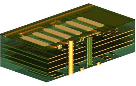
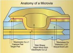
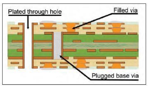
A microvia maintains a laser-drilled diameter of (typically 0.006”, 0.005”, or 0.004”, which are optically aligned and require a pad diameter (typically 0.012”, 0.010”, or 0.008”, allowing additional routing density. Microvias can be via-in-pad, offset, staggered or stacked, non-conductive filled and copper plated over the top or solid copper filled or plated. Microvias add value when routing out of fine pitch BGAs such as 0.8 mm pitch devices and below.
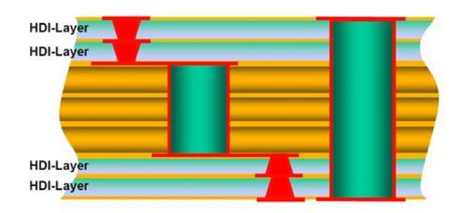
Additionally, microvias add value when routing out of a 0.5 mm pitch device where staggered microvias can be used, however, routing micro-BGAs such as 0.4 mm, 0.3 mm, or 0.25 mm pitch device, requires the use of stacked microvias using an inverted pyramid routing technique.
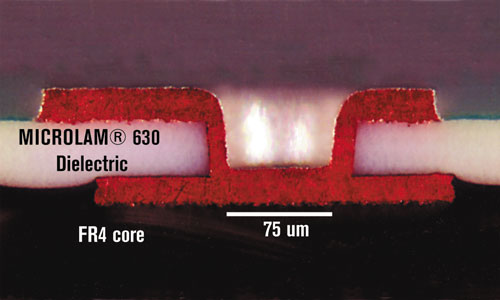
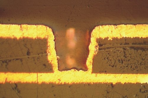
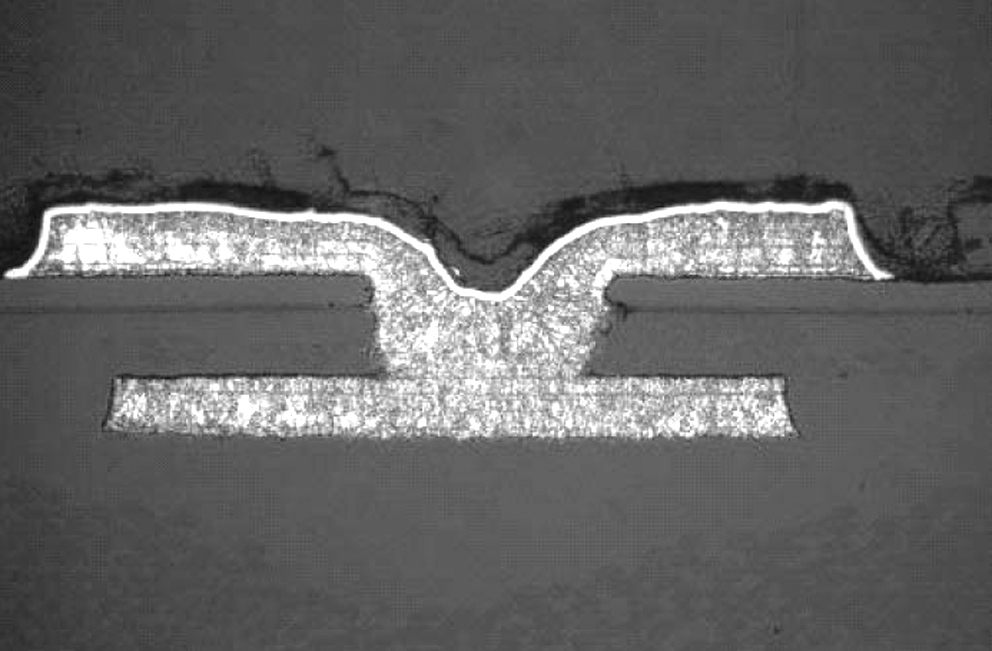
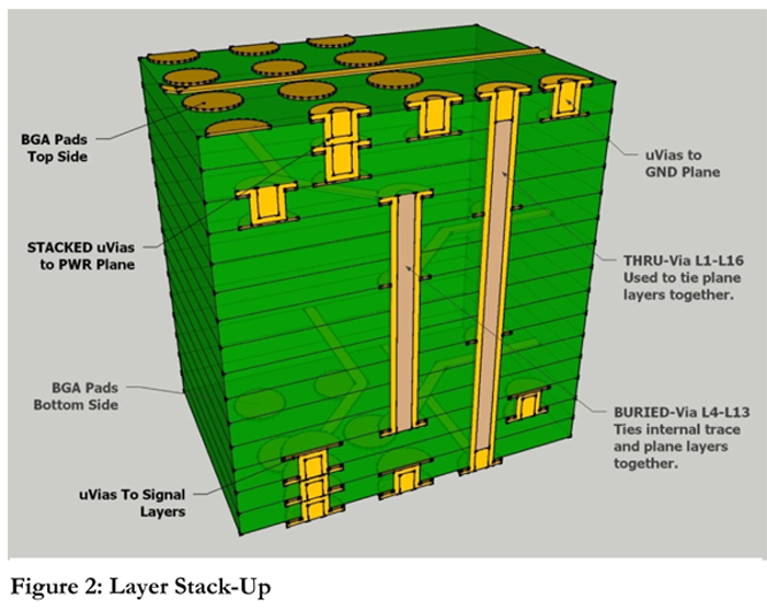
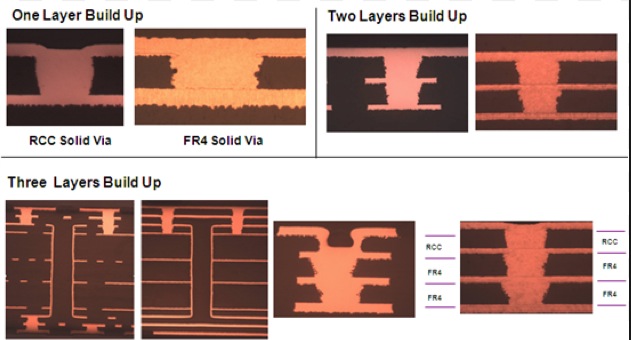
HDI includes the use of fine features or signal traces and spaces of 0.003” (75 µm) or less and laser-drilled blind or buried microvia technology. Microvias allow the use of micro-interconnects from one layer to another within a PWB utilizing a smaller pad diameter creating additional routing density or reducing form factor.
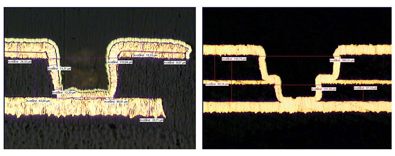
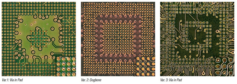
Via in Pad microvias play a decisive role in the miniaturization of circuit boards. “Via in Pad“ means that microvia holes are located directly in the solder pads. As microvias are not blind holes no capillary forces arise. The solder deposit fills the minimum hollow space.